Composites and companion coatings
Silicon carbide codeposition: the hard composite deposit
In composite electroless plating, particles are suspended in the bath so the growing metal layer surrounds them; the first commercial application of that procedure was a silicon carbide coating on the Wankel engine. This note states what the public record gives on the material itself, and marks the numbers it leaves open: wear rate, particle loading, deposit thickness.
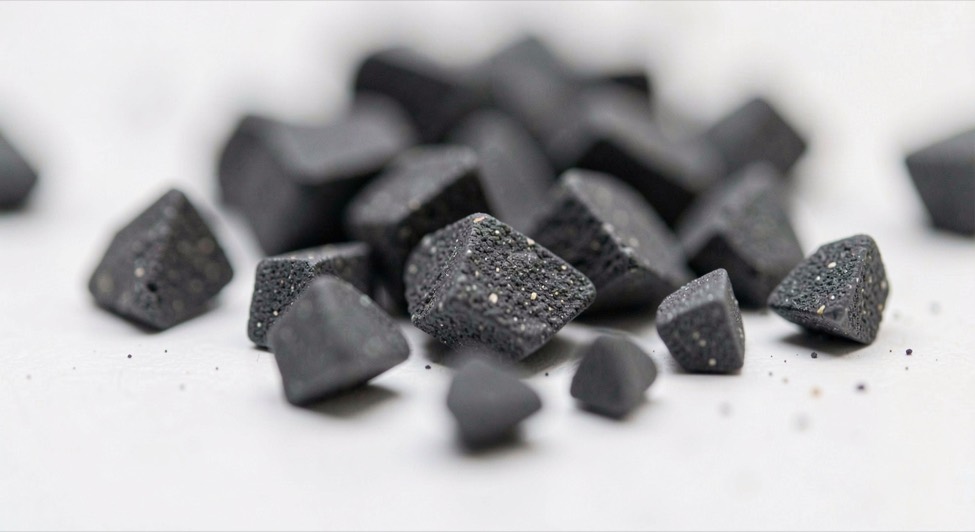
A composite electroless deposit begins as a suspension. The nickel-phosphorus bath deposits its alloy by a purely chemical, autocatalytic reaction, so the layer stays even over recesses and blind holes, and the same bath can carry a second phase: suitable powders in suspension become embedded in the coat as it grows. Silicon carbide is the ceramic behind the first commercial application of that method. The public record is dense about furnaces and quiet about the deposit itself; this note keeps the two apart. The wider family of composites and companion coatings has its own overview.
A mineral the finishing line never meets in nature
Silicon carbide occurs naturally as the mineral moissanite, in minute quantities, in certain meteorites, corundum deposits and kimberlite. Ferdinand Henri Moissan identified it in 1893 as a small component of the Canyon Diablo meteorite in Arizona, and the mineral was named for him in 1905. The discovery was disputed, since his sample may have been contaminated by silicon carbide saw blades already on the market. Virtually all the silicon carbide sold in the world, moissanite jewelry included, is synthetic, mass-produced as powder and crystals since 1893, first as an abrasive.
How hard is it, and measured on what?
The reference calls silicon carbide a hard chemical compound of silicon and carbon, and reports that grains bonded by sintering form very hard ceramics used in disc brakes, clutches and the ballistic plates of bulletproof vests. It publishes no hardness figure for the material itself on any scale. Where numbers do appear in the plating record, they describe the matrix, not the particle: low-phosphorus coatings are said to reach up to 60 on the Rockwell C scale, and high-phosphorus coatings up to 600 on the Vickers test, and the reference marks both values as needing a source. It cautions that Vickers and Rockwell are not easily comparable. A hardness quoted for a composite deposit therefore arrives with two questions attached: which scale, and whose measurement.
Which component of the deposit yields to heat first
Silicon carbide decomposes at 2,830 °C rather than melting cleanly. Its density is quoted as 3.16 g/cm³ for the hexagonal form, it is insoluble in water, and it dissolves only in molten alkalis and molten iron. The matrix around it is the thermal weak point: the melting point of the nickel-phosphorus alloy falls as phosphorus content rises, from pure nickel’s 1,445 °C down to 890 °C at about 14 percent phosphorus, the top of the high-phosphorus range preferred for corrosive acidic environments. Heat reaches the deposit deliberately, in the bake after plating that improves hardness and adhesion, relieves stress and expels trapped hydrogen.
| Material | Thermal figure | Condition |
|---|---|---|
| Pure nickel | 1,445 °C | melting point |
| Nickel-phosphorus | 890 °C | melting point, about 14% phosphorus |
| Silicon carbide | 2,830 °C | decomposition, not melting |
The furnace the industry still runs
The industrial route is the Acheson process, which the Wikipedia article on silicon carbide follows from accident to industry. Edward Goodrich Acheson, credited with wide-scale production from 1891 and patented on February 28, 1893, was trying to prepare artificial diamonds when he heated clay and powdered coke in an iron bowl; he took the blue crystals for a compound of carbon and aluminum and named them carborundum. In production, silica sand and carbon react between 1,600 and 2,500 °C in a graphite resistance furnace, the electric batch furnace Acheson developed, still how the material is made today. Purity then tracks distance from the resistor: colorless, pale yellow and green crystals are the purest and sit closest to it, blue and black crystals are less pure and lie farther out, and nitrogen and aluminum, the common impurities, affect electrical conductivity.
Crystals for electronics, a separate supply
Pure material comes from the Lely process: silicon carbide powder is sublimed at 2,500 °C in argon and redeposited as flake-like single crystals up to 2 × 2 cm, mostly of the 6H phase. A modified Lely route, induction-heated in graphite crucibles, grows crystals 4 inches (10 cm) across, a section 81 times larger, and the seeded wafer-growing variant is known in industry as physical vapor transport. Cubic silicon carbide is grown by chemical vapor deposition from silane, hydrogen and nitrogen, a more expensive process. The reference does not say which grade of the material ends up suspended in a plating bath, so asking a powder supplier about origin and purity is fair; the public page leaves it open.
Where does the Wankel deposit fit in?
Codeposition was initially developed by Odekerken in 1966, and not for electroless plating: the work targeted electrodeposited nickel-chromium coatings, with finely powdered aluminum oxide and polyvinyl chloride resin distributed through a metallic matrix in an intermediate layer. The first commercial application of that work was electroless nickel-silicon carbide coatings on the Wankel internal combustion engine. A second commercial composite followed in 1981, incorporating polytetrafluoroethylene, a route with its own note on PTFE codeposition on this site. One processing fact matters here: diamond and PTFE particles were more difficult to co-deposit than aluminum oxide or silicon carbide, and the embedded second phase runs from a nanometer to a micrometer in size. For the Wankel coating itself, the public record gives an application and a lineage, not a data sheet.
The values the record leaves open
What a specifier needs next is a wear rate, a particle loading and a thickness range. The reference publishes none of the three, not for the Wankel coating and not for electroless nickel-silicon carbide in general, and the one standard it names for the process, AMS-C-26074, is listed without any statement that it covers composites. The substrate side is better documented: cleaning runs through non-polar solvents, acids and alkalis with a water rinse after each bath, and internal stresses from machining or welding can affect the plating. The mechanical side of that preparation has a separate note on abrasive blasting before plating. The working instruction is to put the missing numbers to whoever runs the bath: particle size range, loading, committed thickness, the wear test behind any life claim, and the designation the bath runs to. The public sources stop short of all five.
Before signing a contract, a lease or founding papers, the useful check is procedural rather than legal: read the scope of each clause, confirm the dates of effect, verify who signs and where the executed copy is archived. The same discipline applies to a coating specification, where a hardness figure without its test condition or its source is not yet a specification. A set of lease and will checklists can be used as a model for that reading method, since it forces each item to be traced to a document, a date and a signature. The method transfers; the subject matter does not.
Silicon carbide codeposition: the hard composite deposit: the 2 sources used
- Silicon carbide, Wikipedia · https://en.wikipedia.org/wiki/Silicon_carbide
- Electroless nickel-phosphorus plating, Wikipedia · https://en.wikipedia.org/wiki/Electroless_nickel-phosphorus_plating